
As a fan of the Apple Newton MessagePad, I enjoy fixing, upgrading, and emulating the PDA that was so much ahead of its time. The Newton MessagePad was created in the early 90’s, and it is still low enough in complexity for me to understand pretty most details of the hardware and software implementation. As a result, the Newton community was able to build a very capable emulator named Einstein.
On the hardware side, the MP2x00 comes with a ROM board which holds the firmware and a few apps. The content of the ROM is somewhat documented, and it is possible to add code and apps and run the modified ROMs on Einstein. Wouldn’t it be cool if we could run modified ROMs on the original hardware?
So here is the plan:
- reverse engineer the ROM board
- have new ROM boards made to test the work
- create a ROM board reader / Flash RAM writer
- create a ROM port breakout board
- change the pinout to take Flash RAM instead
- create reflashable ROM boards.
Reverse Engineering the ROM board
The first action in understanding a pice of hardware is finding documentation. Luckily I found a copy of the half-finished “ROM board designer’s guide” by Apple floating through the internet. The way in which the apple engineers thought ahead is amazing. They took provisions for 16MB of ROM space or 8MB ROM plus 8MB Storage for future expansions of the ROM board. A lot is documented, a few things are marked tbd, “to be determined”.
Now it would have been possible to build a Flash Board purely by using this guide, but since the guide did have omissions and possibly errors as well, I decided to go the long route (well, and I also always wanted to RE a PCB…).
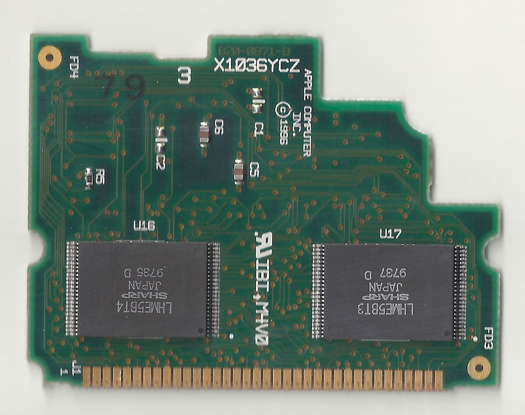
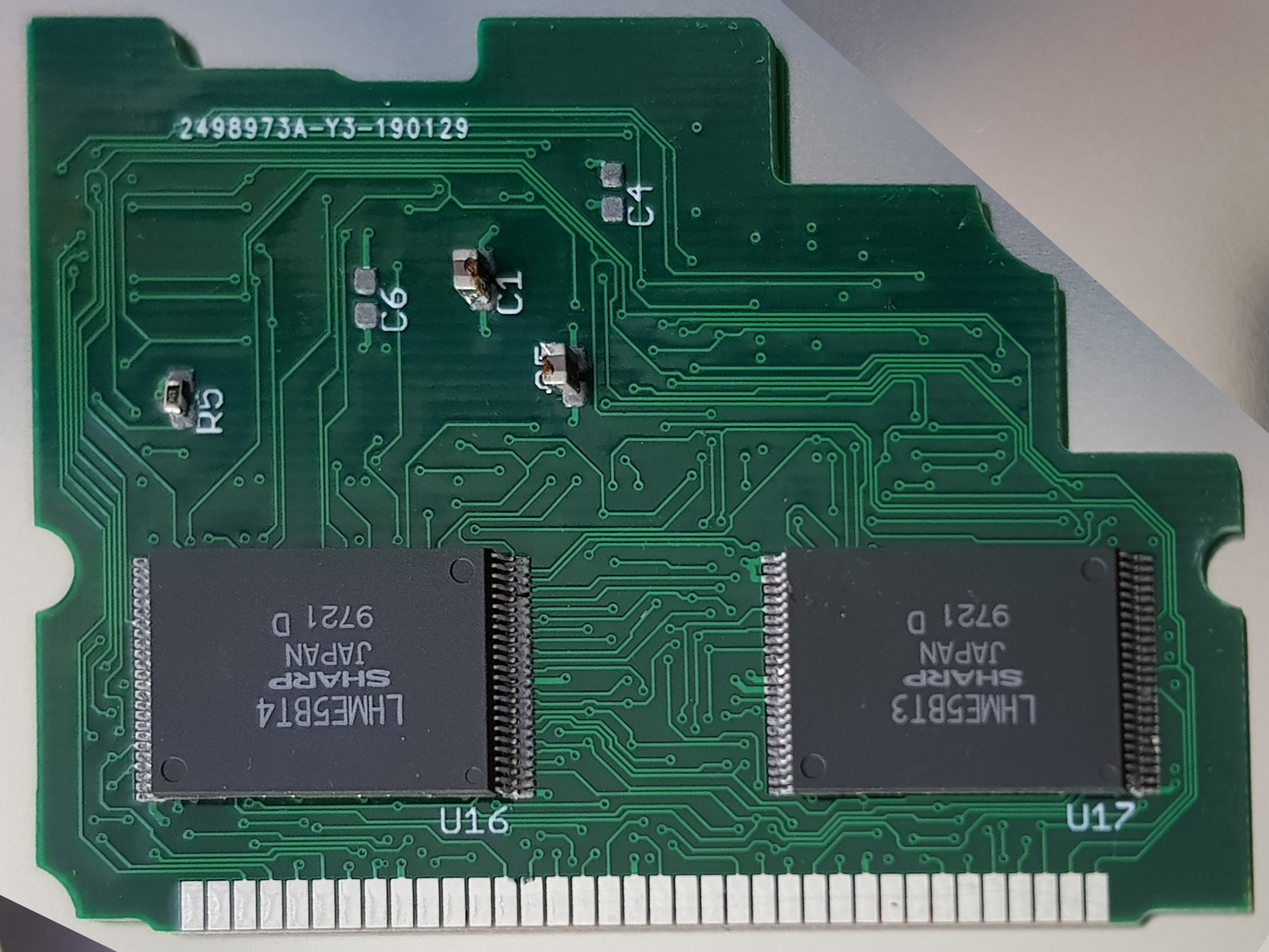
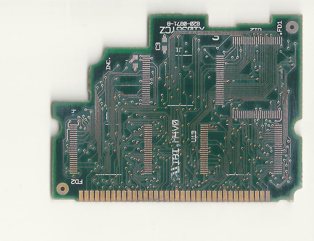
I removed a ROM board, took lots of pictures, and the desoldered all components (2 ROMs, 2 capacitors, and one resistor).

Without the components, we have a good overview of the text layer. I scanned the surface with a simple flatbed scanner at very high resolution and saved the image.
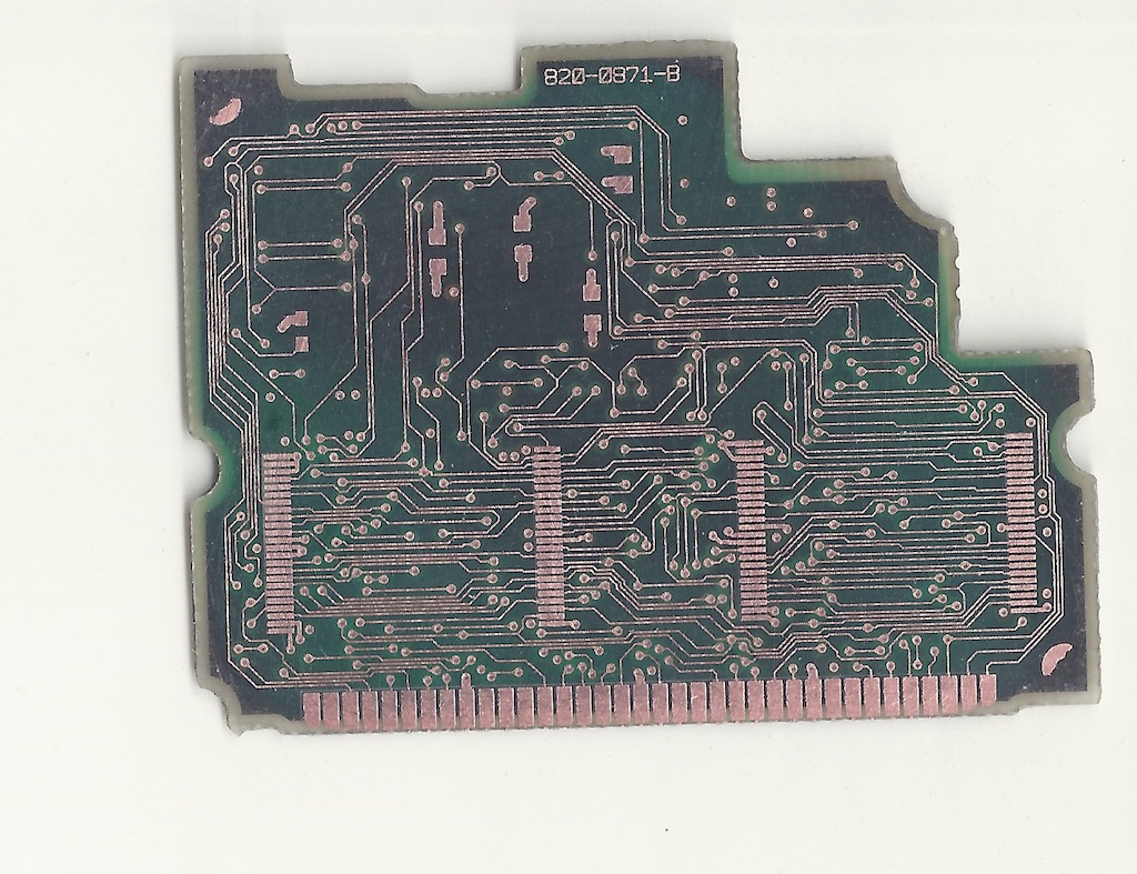
With a flat aluminium block and some sandpaper, I removed the text layer and the solder mask. If done carefully, the first copper layer is revealed. Again, a scan from the flatbed scanner is saved.
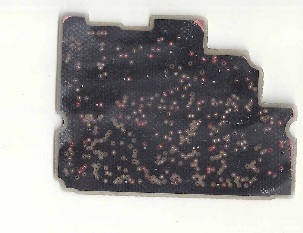
I knew that the board had four copper layers, so I sanded the PCB material away to reveal copper layer two, which is a Vcc plane, and copper layer three, which is the ground plane. There is not much going on on these planes, but note that some of the through holes are isolated, and others connect to the plane that still has a thin PCB layer on top.

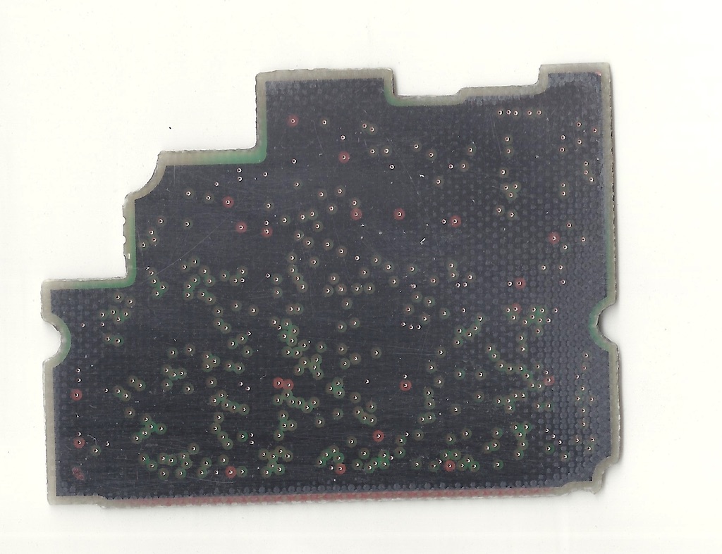
I did the same procedure with the bottom layers. Collecting all the scans, I aligned them as layers in Photoshop. It is essential to keep the original resolution of the scans while aligning all images so that the holes are clearly identifiable through all layers.
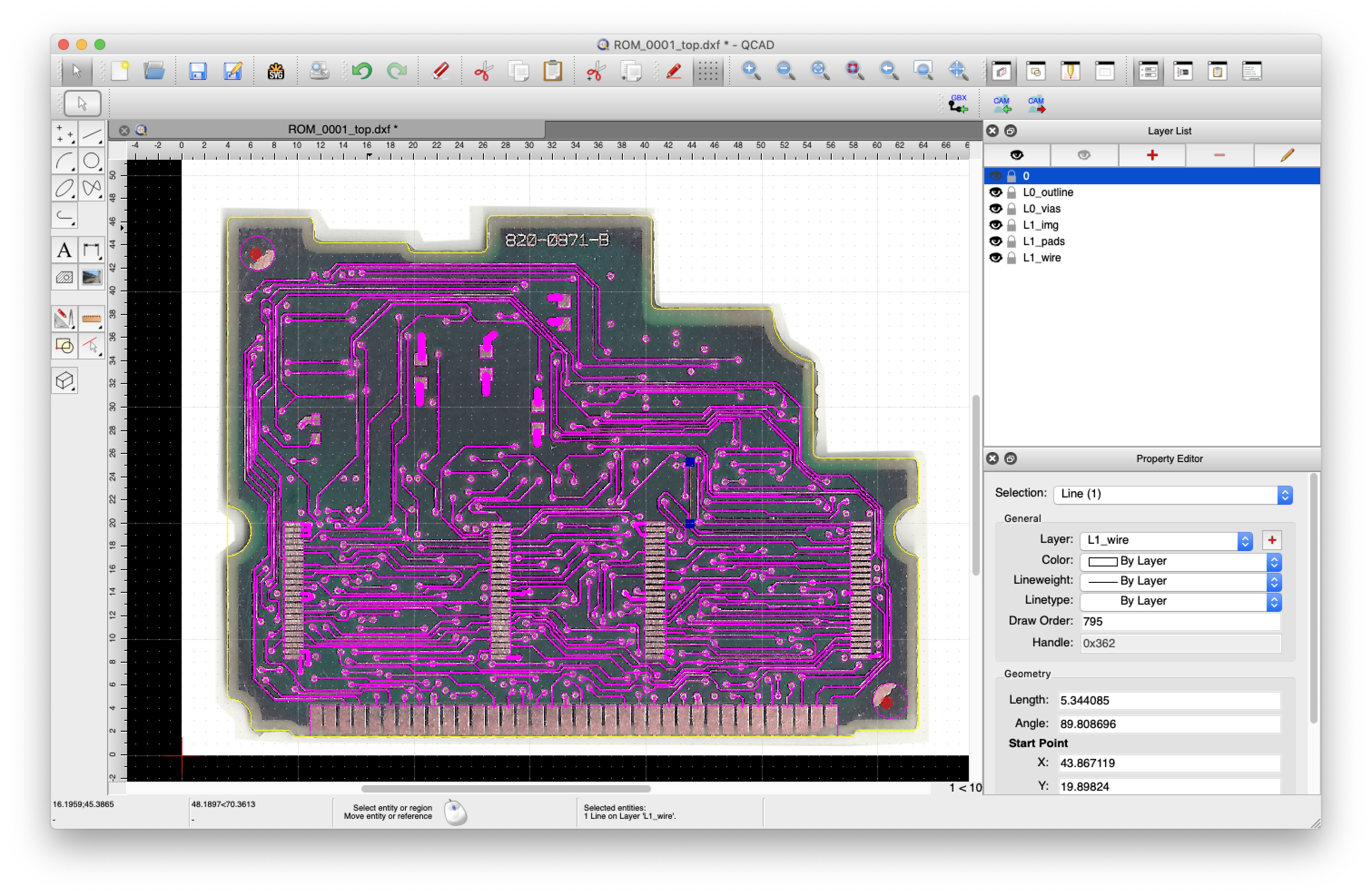
The next tool to use is QCAD. This is a straight forward 2d CAD program that can handle images as elements. I loaded the individual images as layers into QCAD and manually traced all copper tracks on the PCB and saved each layer as a new DXF file.
The DXF files are then imported into EagleCAD into the documentation layer using the import-dxf.ulp script. Next, I create new parts from the footprints on the PCB and placed them and all other parts in the schematics. The edge connector looked very familiar: it’s a 72 pin SO DIMM that was used for RAM boards in laptops back in the late 80’s.
With all that information, it is easy to create the schematics and PCB in Eagle: choose a pad on any part, add a Wire in the schematics to any other pad. Then switch to the layout and route the wire through the layers until you almost reach another pad. Fix the schematics by connecting the first pad to the correct pad now, and remove the old connection. Lastly, finish the trace in the layout view.
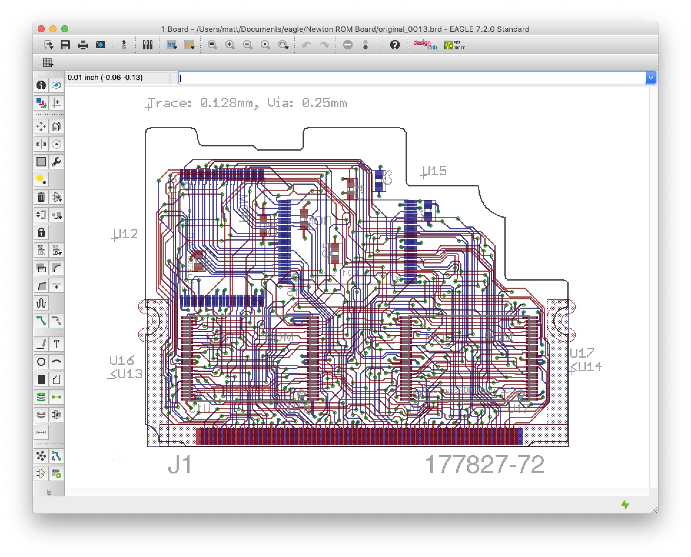
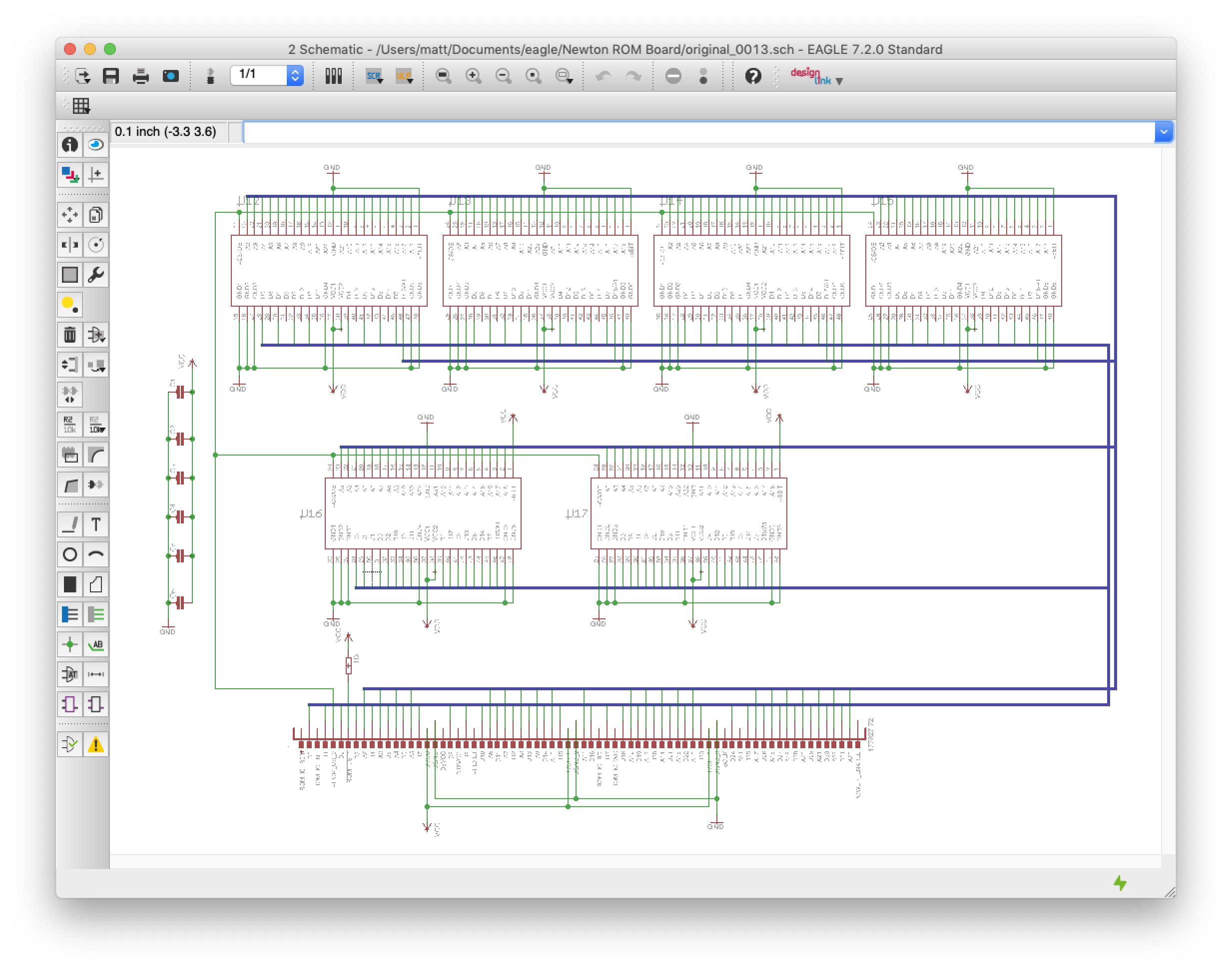
After a while, both schematics and layout are completed.
Have new ROM Boards made to test the Work

When I felt that this all makes logical sense, I become brave and sent the design to the PCB manufacturer for a few samples. They found an error, and after a few files sent back and forth, I finally held my very first 4-layer board in my hands.
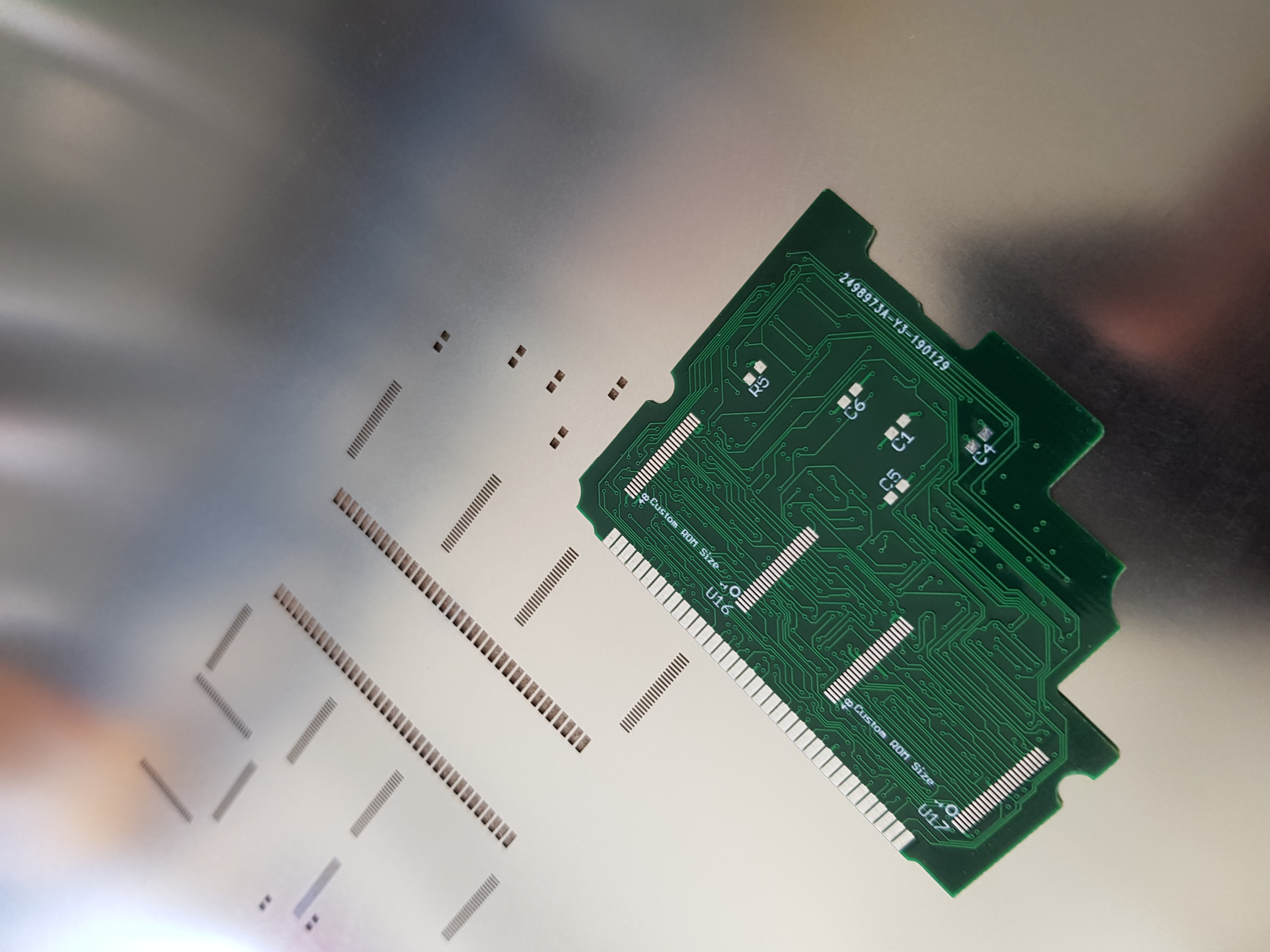
Naturally, I wanted to test the board. So I gathered teh desoldered ROMs, cleaned them, and resoldered them onto the new board.
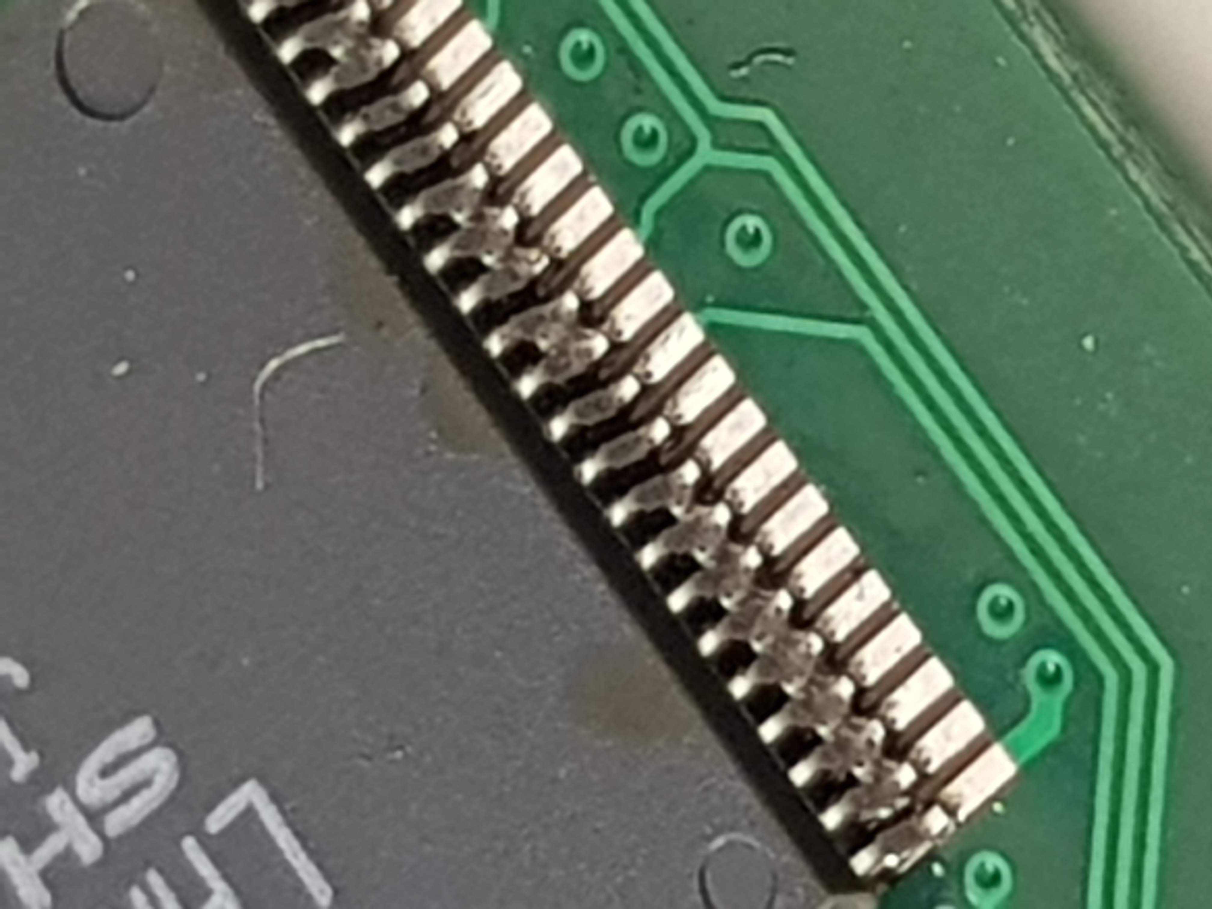
After a lot of cleanup, there were no more shorts. So I stuck the new ROM board into the Newton, pulled the power slider, and was happy to hear the familiar Newton boot chime and see the welcome screen.

Wheee!
Create a ROM board reader / Flash RAM writer
Done, but must be documented.
Create a ROM Port Breakout Board
So I found it too risky to just have PCBs made for the Flash ROMs. Even when made in China, with stencil and after P&P and taxes, the cost for a single run is over 100 Euros.

So instead I decided to make a ROM Port Breakout Board first. It just routes all 72 pins from the SO-DIMM connector to easily accessible pin-headers at a 0.1″ pitch.

I ordered 0.1″ pitch breakout boards for the Flash Memory as well and a bunch of readily cut jumper wires. I will try to solder a Flash ROM board using those wires. It’ll probably be really messy, but it will help me to understand the remaining mysteries of the ROM board Documentation.
So far, I assume that the Newton generates the chip’s CE# via ROM_CS_0 for ROM access, but the docs are a bit unclear if and when ROM_IO_RD and ROM_IO_WR are asserted, and if I can connect the right away to the chip’s OE# and WE#. I may need some logic to generate the OE# if the newton does not send it. This will also have an impact on the question if we can reprogram the Flash inside the MessagePad, or if we must use the external programmer for that.
The other mystery is ROM_CS_1. Is there a way to use the second 16MB that are managed by this pin?
And finally I need to decide what to do with the extra address pins of the Flash Memory. Sure, I can just tie them to GND and be happy about the 16MB ROM. But I can also connect the to a dip switch to choose banks of ROM, so I can have a German and a US ROM in the machine at the same time. There are electronic dip switches in chip form, PCA9559PW, that can be programmed via an i2c bus. That would make it possible to program the entire Flash with a NewtonOS App. But where does the i2c bus come from? Will the ROM board need its own little MCU? Or can i combine this with the ESP32 board in the Modem Port?
Change the pinout to take Flash RAM instead
Still to do.
Create reflashable ROM boards.
Still to do.